- 您现在的位置:买卖IC网 > Sheet目录471 > MAX19994AEVKIT# (Maxim Integrated)KIT EVAL FOR MAX19994A MIXER
�� �
�
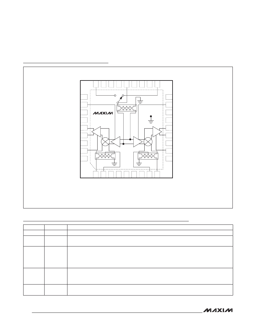
�Dual,� SiGe,� High-Linearity,� 1200MHz� to� 2000MHz�
�Downconversion� Mixer� with� LO� Buffer/Switch�
�Pin� Configuration/Functional� Block� Diagram�
�TOP� VIEW�
�27�
�26�
�25�
�24�
�23�
�22�
�21�
�20�
�19�
�N.C.�
�LO_ADJ_M�
�28�
�29�
�18�
�17�
�N.C.�
�LO_ADJ_D�
�V� CC�
�IND_EXTM�
�IFM-�
�IFM+�
�GND�
�IFM_SET�
�V� CC�
�30�
�31�
�32�
�33�
�34�
�35�
�36�
�MAX19994A�
�EXPOSED� PAD�
�16�
�15�
�14�
�13�
�12�
�11�
�10�
�V� CC�
�IND_EXTD�
�IFD-�
�IFD+�
�GND�
�IFD_SET�
�V� CC�
�+�
�1�
�2�
�3�
�4�
�5�
�6�
�7�
�8�
�9�
�TQFN�
�(6mm� � 6mm)�
�EXPOSED� PAD� ON� THE� BOTTOM� OF� THE� PACKAGE�
�Pin� Description�
�PIN�
�1�
�2�
�3,� 5,� 7,�
�12,� 20,�
�22,� 24,�
�25,� 26,� 34�
�4,� 6,� 10,�
�16,� 21,�
�30,� 36�
�8�
�22�
�NAME�
�RFMAIN�
�TAPMAIN�
�GND�
�V� CC�
�TAPDIV�
�FUNCTION�
�Main� Channel� RF� input.� Internally� matched� to� 50� I� .� Requires� an� input� DC-blocking� capacitor.�
�Main� Channel� Balun� Center� Tap.� Bypass� to� GND� with� 39pF� and� 0.033� F� F� capacitors� as� close� as�
�possible� to� the� pin� with� the� smaller� value� capacitor� closer� to� the� part.�
�Ground�
�Power� Supply.� Bypass� to� GND� with� capacitors� as� close� as� possible� to� the� pin,� as� shown� in� the�
�Typical� Application� Circuit� .�
�Diversity� Channel� Balun� Center� Tap.� Bypass� to� GND� with� 39pF� and� 0.033μF� capacitors� as� close� as�
�possible� to� the� pin� with� the� smaller� value� capacitor� closer� to� the� part.�
�发布紧急采购,3分钟左右您将得到回复。
相关PDF资料
MAX19995ETX+T
IC DOWNCONVERTER 2CH 36TQFN
MAX19995EVKIT#
EVALUATION KIT FOR MAX19995
MAX19996AEVKIT#
EVALUATION KIT FOR MAX19996A
MAX19996ETP+T
IC MIXER DOWNCONV 20-TQFN-EP
MAX19997AETX+T
IC DOWNCONVERTER 2CH 36TQFN
MAX19998ETP+
IC MIXER DOWNCONVERSION 20TQFN
MAX19999ETX+T
IC DOWNCONVERTER 2CH 36TQFN
MAX2009ETI+T
IC RF PREDISTORT ADJ 28-TQFN
相关代理商/技术参数
MAX19995AETX+
功能描述:上下转换器 High-Gain 1.2GHz to 2GHz Downconv RoHS:否 制造商:Texas Instruments 产品:Down Converters 射频:52 MHz to 78 MHz 中频:300 MHz LO频率: 功率增益: P1dB: 工作电源电压:1.8 V, 3.3 V 工作电源电流:120 mA 最大功率耗散:1 W 最大工作温度:+ 85 C 安装风格:SMD/SMT 封装 / 箱体:PQFP-128
MAX19995AETX+T
功能描述:上下转换器 High-Gain 1.7GHz to 2.2GHz Downconv RoHS:否 制造商:Texas Instruments 产品:Down Converters 射频:52 MHz to 78 MHz 中频:300 MHz LO频率: 功率增益: P1dB: 工作电源电压:1.8 V, 3.3 V 工作电源电流:120 mA 最大功率耗散:1 W 最大工作温度:+ 85 C 安装风格:SMD/SMT 封装 / 箱体:PQFP-128
MAX19995AEVKIT#
功能描述:射频开发工具 RoHS:否 制造商:Taiyo Yuden 产品:Wireless Modules 类型:Wireless Audio 工具用于评估:WYSAAVDX7 频率: 工作电源电压:3.4 V to 5.5 V
MAX19995ETX+
功能描述:上下转换器 High-Gain 1.7GHz to 2.2GHz Downconv RoHS:否 制造商:Texas Instruments 产品:Down Converters 射频:52 MHz to 78 MHz 中频:300 MHz LO频率: 功率增益: P1dB: 工作电源电压:1.8 V, 3.3 V 工作电源电流:120 mA 最大功率耗散:1 W 最大工作温度:+ 85 C 安装风格:SMD/SMT 封装 / 箱体:PQFP-128
MAX19995ETX+T
功能描述:上下转换器 High-Gain 1.7GHz to 2.2GHz Downconv RoHS:否 制造商:Texas Instruments 产品:Down Converters 射频:52 MHz to 78 MHz 中频:300 MHz LO频率: 功率增益: P1dB: 工作电源电压:1.8 V, 3.3 V 工作电源电流:120 mA 最大功率耗散:1 W 最大工作温度:+ 85 C 安装风格:SMD/SMT 封装 / 箱体:PQFP-128
MAX19995EVKIT#
功能描述:射频开发工具 RoHS:否 制造商:Taiyo Yuden 产品:Wireless Modules 类型:Wireless Audio 工具用于评估:WYSAAVDX7 频率: 工作电源电压:3.4 V to 5.5 V
MAX19996AETP+
功能描述:上下转换器 High-Gain 2GHz to 3.9GHz Downconv RoHS:否 制造商:Texas Instruments 产品:Down Converters 射频:52 MHz to 78 MHz 中频:300 MHz LO频率: 功率增益: P1dB: 工作电源电压:1.8 V, 3.3 V 工作电源电流:120 mA 最大功率耗散:1 W 最大工作温度:+ 85 C 安装风格:SMD/SMT 封装 / 箱体:PQFP-128
MAX19996AETP+T
功能描述:上下转换器 High-Gain 2GHz to 3.9GHz Downconv RoHS:否 制造商:Texas Instruments 产品:Down Converters 射频:52 MHz to 78 MHz 中频:300 MHz LO频率: 功率增益: P1dB: 工作电源电压:1.8 V, 3.3 V 工作电源电流:120 mA 最大功率耗散:1 W 最大工作温度:+ 85 C 安装风格:SMD/SMT 封装 / 箱体:PQFP-128